Main page
About us
Sliding Bearings Consulting
Advertising Opportunities

to Metals
to Metallographic examination
Scanning Electron Microscope
Dr. Dmitri Kopeliovich
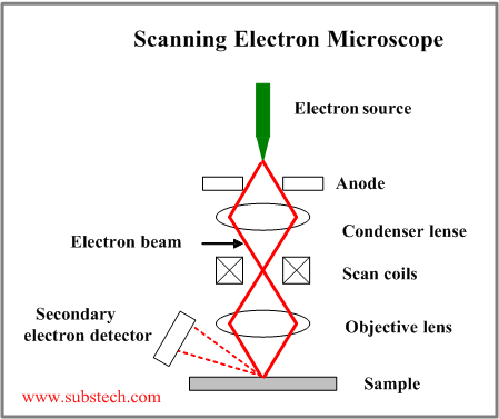
Scanning Electron Microscopes (SEM) use focused beam of electrons, scanning in vacuum the specimen surface, imaging one point at a time.The interaction of the electron beam with every point of the specimen surface is registered, forming the entire image.
Since the wavelength of the electron beam is much lower than wavelength of the visible light, the magnification of SEM is much higher (thousands of times), than that of optical microscopes.
Resolution of SEM is about 1nm to 20 nm.
Electrons in the electron gun are emitted from the cathode and accelerated by the anode to the energy 1 – 50 keV.
The electron beam is condensed by the condenser lenses (one or two).
Magnetic field, produced by the scan coils deflects the electron beam back and forth.
The electron beam, focused by the objective lens to very fine spot (1-5 nm), scans the sample surface in a raster pattern.
Primary electrons interact with the atoms of the sample surface, causing emissions of the secondary electrons, which are detected, producing the image.
The backscattered electrons of the electron beam may also be detected.
The backscattered electron image is used for contrasting the sample regions, having different chemical compositions.
X-Ray Microanalysis
Interaction of the electron beam with the specimen atoms results in emission of x-rays, which are detected and analyzed by X-Ray Spectroscope. This allows to produce qualitative and quantitative analyses of the different regions of the sample.
to top
Related internal links


